Τεχνικό φυλλάδιο
Προδιαγραφές
Brand
AlteraKit Contents
Ribbon Cable
Kit Type
ByteBlaster II Parallel Port
Standards/Approvals
No
Product Type
Programmers & In-Circuit Emulator
Sub Type
Programmer
For Use With
Altera Device
Χώρα Προέλευσης
Taiwan, Province Of China
Λεπτομέρειες Προϊόντος
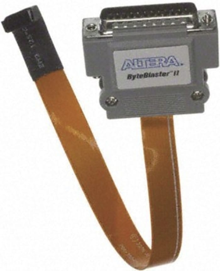
The ByteBlaster™ II download cable allows you to program and configure Altera devices. This cable drives configuration data from a standard parallel printer port on a PC to the device on the PCB. Because design changes are downloaded directly to the device, prototyping is easy and you can accomplish multiple design iterations in quick succession.
An FPGA is a semiconductor device consisting of a matrix of Configurable Logic Blocks (CLBs) connected through programmable interconnects. The user determines these interconnections by programming SRAM. A CLB can be simple (AND, OR gates, etc) or complex (a block of RAM). The FPGA allows changes to be made to a design even after the device is soldered into a PCB.
Ημερομηνία αποθέματος προσωρινά μη διαθέσιμη
€ 308,62
€ 308,62 Μονάδας (Exc. Vat)Χωρίς Φ.Π.Α
€ 382,69
€ 382,69 Μονάδας Με Φ.Π.Α
1
€ 308,62
€ 308,62 Μονάδας (Exc. Vat)Χωρίς Φ.Π.Α
€ 382,69
€ 382,69 Μονάδας Με Φ.Π.Α
Ημερομηνία αποθέματος προσωρινά μη διαθέσιμη
1
Τεχνικό φυλλάδιο
Προδιαγραφές
Brand
AlteraKit Contents
Ribbon Cable
Kit Type
ByteBlaster II Parallel Port
Standards/Approvals
No
Product Type
Programmers & In-Circuit Emulator
Sub Type
Programmer
For Use With
Altera Device
Χώρα Προέλευσης
Taiwan, Province Of China
Λεπτομέρειες Προϊόντος
The ByteBlaster™ II download cable allows you to program and configure Altera devices. This cable drives configuration data from a standard parallel printer port on a PC to the device on the PCB. Because design changes are downloaded directly to the device, prototyping is easy and you can accomplish multiple design iterations in quick succession.
An FPGA is a semiconductor device consisting of a matrix of Configurable Logic Blocks (CLBs) connected through programmable interconnects. The user determines these interconnections by programming SRAM. A CLB can be simple (AND, OR gates, etc) or complex (a block of RAM). The FPGA allows changes to be made to a design even after the device is soldered into a PCB.